
Our developments rest on self-made technology base
In: «Nizhegorodskii Potential' journal of the Nizhny Novgorod Research Center RAS, № 3, 2011
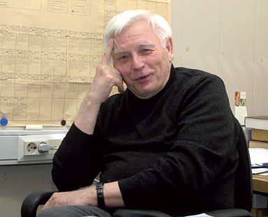
Today’s guest of our 'Formula of success' column is head of multilayer x-ray optics department with IPMRAS, laureate of the USSR State Prize and of the RAS Stoletov Prize, corresponding member of the Russian Academy of Science, doctor of physical and mathematical sciences, Nikolai Nikolayevich Salashchenko.
 — When people referred to as «the children of war' talk about those times, they would recall some bright moments of their childhood rather than hardships. Nikolai Nikolayevich, which of your early years experiences do you remember most?
— That I did not recognize my father when we first met.
You see, I was born in Ussuriisk on November 1, 1941, when my father, career army officer, was already fighting on the Western front. I was named Nikolai because there was no news of him. In this way my mother apparently tried to help him, as she would frequently mention this name. I first saw father in 1947 in Berlin where he served, when the officers' families were allowed to join them. I remember that father failed to meet us because he was coming from Leipzig and was late. We were met by some officer who escorted us to the officers' apartment building. I was tired and fell asleep, and when I woke up I saw a few military men who looked alike and pretty adult to me. Of course, it was a child’s perception, in fact, they were a little over thirty at the time. Suddenly one of them laughed and said, «Come on, pick out a dad!'. Since I had never seen him, I got shy and hid behind mother’s back. I was proud of my father. He was a good commander of regiment, I know it. Once I found a war-time photograph that pictured three soldiers who I would say looked rather advanced in age, and on the reverse side there was an inscription: «To our favorite commander'.
In two years we moved from Germany to Omsk. The military are always on the go — I changed many schools. And after the 8th grade, on 7 June 1957, at fifteen I was employed at a defense plant (it seemed there were no other industries back then), first as a turner’s apprentice and then as a turner, but since I worked in the experimental shop, I was bound to master practically every kind of machine tool in it besides a turning lathe. At the same time I studied at an evening school.
— Why evening school?
— I can’t even say. It was quite unexpected for my parents because when I made that decision they were away. And when I met them at the station I just said I was short of time because I had to go back to work and suggested we talk about it later in the evening. Had they been at home, they would probably not have allowed me to make such a turn. But not only I did this. Our life was not that easy, and the general atmosphere, like people going to develop virgin lands — it all had a certain influence on me. May be, it is my retrospective view of the situation, but it was so.
Anyway, I keep warmest memories of the evening school. There were people of different ages in the class and we all were very friendly. I was just 15, the youngest in the group. I didn’t even have a passport, they took me on at the plant based on the birth certificate. Among the students were workers, foremen, and even a militia captain, Ivan Levchenko. We became good friends, although he was older, with the experience of the war. We had common life, and the age difference did not seem to matter: in the morning we all went to work and evenings met at school and shared the problems it posed. It was real fraternity!
— Your major school was at the plant, wasn’t it?
— It was not a school of life, it was real adult life itself at the plant. The shop I worked in was experimental, everyone was to be able to operate all the machinery there was in it. My master, fitter-mechanic Grigorii Mitrofanovich Mazanov who taught me all the tricks of the working craft, was an academician in terms of workmanship. People from different places came to him for advice and training. A professional of such a level of competence at that time got a salary as high as a minister’s.
The workers in our shop were assigned to designers, but it seemed to me it was the other way round because the designers used to ask our advice about a feasibility and technology of fabrication оf a certain part or node, they left the drawing and you were free to do whatever you liked with it provided you’d turn out a model! Of course, it flattered me, for I was only a boy. And I would spare no pains to save face. The versatile technical skill and experience I acquired at that factory serves me all my life.
— What was your life like in the following years? Where did you get higher education?
— After finishing school in 1959 I considered applying to the Omsk Institute for machine building, device construction department, but they did not open this faculty and so I chose the area I had been working in for over two years already, i. e., the department for metal cutting machines and tools. And was admitted. Although I was a full-time student, the first three terms we were supposed to simultaneously work at Sibzavod (the Siberian plant). It was a three-shift work included in our curriculum schedule. I have a school friend, Yu. K. Verevkin, now a leading scientist at IAP RAS, with whom we studied together at this institute. I think, we would have become machine building engineers, as originally intended, if it hadn’t been for a sudden turn in our life.
In 1962 Yury and I were selected for a course of training in radiophysics, so that upon completion we would teach radio science and engineering at the new faculty for radio engineering, opened at the institute in Omsk. The course was offered by different institutions of higher education; Yury, me and Volodya Razborov (now a docent at the Technical University of Nizhny Novgorod) were sent to the Polytechnical institute in Gorky, and we were enrolled for a course below the level of the one we were eligible to. We took our future teaching profession very seriously: in addition to the classes in Polytech we attended many lecture courses at the radiophysics department of the University. Moreover, we started working at different faculties including the departments for radio receiving and transmitting devices. In our third or fourth year of study, we once had the nerve to tell А. V. Gaponov-Grekhov after his lecture that we would like to work with him. He was a little taken aback but said he would think it over. And indeed, in a while Andrey Viktorovich placed us with V. I. Talanov (at present academician of RAS). By that time we had already listened to his special course on open cavities at the university and were more or less ready to talk. V. I. Talanov became our diploma projects supervisor.
After defending the diplomas we were invited by Mikhail Adolphovich Miller who offered to leave us for work at the Radiophysics Research Institute, NIRFI. We quailed at the thought for we were bound to get back to Omsck, and turned to Andrey Viktorovich, a standard of high morals to us, for advice. He said he would go back, if he were in our place because people were waiting and hoped for our return. And so we came back to Omsk to teach…
— And what about science?
— Of course, in Gorky we had «caught the virus' and looked forward to continuing the research activities. The faculty in Omsk was new and understaffed, and in three years I had to master and conduct courses in seven different disciplines. I still am ashamed for that «professor. On the other hand, it was a kind of self-education for me.
When three years later I returned to Gorky in 1968, there were no vacancies in NIRFI and so I landed a job at the SALUTE research and production enterprise, in the department headed by Vladimir Zinovievich Vysotsky. We happened to work in one lab with Sergey Viktorovich Gaponov who became my immediate chief. G. A. Domrachev, corresponding member of RAS, also worked there back then. So, the department led by V. Z. Vysotsky turned out three Academy members. I was doing pretty well in science and the time came to think of a dissertation, but in 1970, already overage, I was drafted into the army. I left for Ventspils and served two years as a lieutenant in the air defense forces.
I got back to «Salute\' in 1972 and engaged in a brand-new area of research on laser deposition of semiconductors. In 1975 I defended my Ph. D. thesis in this field. My scientific supervisor was professor I. A. Karpovich.
In 1978 a large group of the «Salute\' researchers (about 10-12 people) along with their equipment moved in with the Institute of Applied Physics of the USSR Academy of Science and organized a new department that was headed by Sergey Viktorovich Gaponov.
— How did you and your colleagues survive through the 90s?
— The late 1980s and early 90s saw a boom in the high-temperature superconductivity research. The group led by S. V. Gaponov I was involved with did very well in this field, and therefore it was decided to set up a special design and technology bureau at IAP RAS and even in the department of solid-state physics with a view to solution of applied problems of HTSC. And when the construction of a new building was completed, the decision was made in September 1993 about organization of a new academic institute, the Institute for Physics of Microstructures RAS, on the basis of the IAP department of solid-state physics. The country entered, or was already going through a very hard period, while we were rapidly developing. At least, in the x-ray optics field. Back then, in the absence of state orders many industrial enterprises had to become more responsive to our orders, which allowed us to develop the technology and measuring base on a very tight budget. As a matter of fact, you cannot buy most of the equipment for research in this area (let alone our lack of funds at those times to buy it with). In the early 90s we were already able to do things that no one in the world, or very few, were capable of doing. We started cooperating with other countries, among the first were The Netherlands and Germany. It helped us gain the insights not only into the problems of fundamental science in the field of multiplayer x-ray optics, but also into the needs of a developed industry. We still are involved in active cooperation with both research and industrial companies from several countries.
- But it was the time when many scientists were leaving the country. Was IPM RAS affected?
— Of course, part of our scientists, fairly successful and active ones, had left, unfortunately. However, besides a certain loss incurred by the institute initially, this brain drain proved to be useful in the long run, for it largely contributed to expanding of our scientific contacts. Not only with our ex-associates, but also with many active scientists from other institutes across Russia. We have established close scientific relations with a number of leading research and production centers. At present some ties with our ex-associates have weakened, some, on the contrary, have become stronger and broader. As for me, I didn’t even consider emigration, although I had some offers.
— The institute for physics of microstructures is unlike any other research institute in town. Did you, too, take part in its organization?
— Our institute is the brainchild of Sergey Viktorovich Gaponov. His idea was to create an European-level research institute. As I said, we first had a special design and technology bureau (SKTB) organized for conducting applied research in the area of high-temperature superconductivity, and only after the SKTB building construction was completed the decision was made to establish a new institute.
— Тoday you are a prominent scientist, an internationally known expert in x-ray optics. You are involved in a cutting-edge research pursuing technological breakthroughs into the shortwave range. And where do such ideas come from?
— We do research on multilayer optics for the spectral region of 0.01nm to 100 nm (the 104 range), i. e., the actual wavelength range of our developments extends from hard x-rays to extreme ultraviolet radiation. This scale can be compared only with the scale of operating wavelengths in radio physics (UV to microwaves). Many fundamental problems we deal with arise through solution of specific applied tasks. Our interaction with some leading companies in the field of projection shortwave lithography keeps us in the know about the element and node requirements to lithography stands. And my instant reaction to such standards had always been — «It\'s impossible'. Then, it not only proved possible but we appeared to be the first to have met those requirements, at least in part. Generally speaking, day-by-day achievements in science and technology equip people for solving amazing problems. Mankind has obviously accumulated sufficient fundamental and technological basis to make that possible. Аnd the found solutions enable us to rapidly move on.
But it has to be called for by the society’s needs, there should be a relevant industry working. It is a problem in today’s Russia. Therefore, we value our cooperation with the Rosatom enterprises on whose orders we develop a projection x-ray lithography stand. Extremely important for us is interaction with the ASMLithography, the leading company for development and production of modern lithography equipment. For them we develop multilayer spectral filters for lithography stands, that have no analogs in the world. The developed principles and technologies of spectral filters fabrication are widely used towards x-ray telescopes for imaging of the Sun, and for x-ray diagnostics of high-temperature plasma.
 We are currently involved in development of multilayer optics for the next-generation lithography systems. Today’s new lithography stands for a 13.5 nm operating wavelength have a space resolution of 22 nm, the next step on this way is to achieve 11 nm resolution. At the same time, research and development activities are underway towards multilayer optics for a 6.7 nm wavelength for projection lithography stands with a space resolution to 8 nm. I should say that multilayer optics of such quality does not exist yet and there are no developed technologies for preparing surfaces of a still higher degree of smoothness for mirrors that must be shaped to precision unattainable today. But we will do that, no doubt about it. I'd like to point out that to ensure superhigh resolution imaging of objects in such a short wavelength range we need optical elements with supersmooth surfaces shaped to a precision of fractions of nanometer, and optical systems whose aberrations do not exceed fractions of nanometer, either.
To effect shape control of optical surfaces (spherical and aspherical) with subnanometer precision we have developed a laboratory model of a special interferometer. Such a device in a variety of modifications would be of use at enterprises of the precision mechanics and optics industry in Russia. Since it is unavailable at the world’s high-technology market, the interferometer of this kind can make a success. We are now negotiating a joint development of industrial modifications of our interferometer with a mechanics-and-optics enterprise. But this is only part of our offer to the industry in terms of developments of precision supersmooth optics for any spectral range. The challenge we face is to work out a technology for supersmooth polishing and roughness control of optical surfaces and the techniques for shape correction of surface with subnanometer precision.
At IPM RAS we work out the entire complex of technologies for optical surface preparation. However, to successfully solve the relevant R&D problems and have the new developments promoted to industry, we currently discuss (and, it seems, quite successfully) cooperation opportunities with the research-and-production associations of the Roskosmos Federal space agency and Minprom (the Ministry of Industry and Trade).
Today we make a wide variety of x-ray optical elements for the wavelength range I mentioned: «hard\' x-ray optics for the x-ray structural analysis, elemental analysis (imaging optics and lithography) and x-ray microscopy applications, and we are the only R&D group in the world to produce multilayer spectral filters.
— The IPM RAS achievements in x-ray optics have earned worldwide recognition, the institute is involved in the international scientific cooperation. Are there any research-supporting programs in Russia?
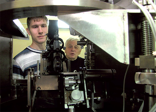
— I have to admit, unfortunately, that in Russia there are no programs to support research on such a large scale. But they work in the world, and we are involved. And we prove to be better in some things, and even the only ones sometimes. In Russia we are supported by the Rosatom and, as I said earlier, different cooperation projects are being discussed now with the Roskosmos and Minprom organizations. But this has nothing to do with a truly nationwide government program. Without such programs it is impossible to realize a systematic approach in carrying out research in a certain area. They believe in ministries that the country will acquire all the necessary means when the need arises. But it would be outdated equipment, which suggests that our industry (what remains of it) will keep lagging behind. Almost all high-tech equipment required for our developments we make ourselves. And IPM RAS is the world’s only institute to have a continuously developing technology and research chain in the area of multilayer x-ray optics.
In this context our involvement in the international programs is very important to us. When you work on some particular parts and components of a device, you have to have a clear idea of the device as a whole, and in this respect our collaboration with foreign colleagues is a great help. To be specific, our current activities for development of next-generation x-ray optics devices are supported by cooperation with the world’s best company-manufacturer of lithography equipment in Holland.
— What issues, do you think, should be of prime consideration for young people who decided to devote themselves to science?
— Good education in the first place, absolutely. Any education proves insufficient the next day, one has to be learning all the time, learning by solving novel problems offered by science. One should be driven by natural curiosity.
As an experimenter, I sometimes (quite often, as a matter of fact) am pained to see young people shirk experimental work, the «metalwork\'. They think that in theoretical research one is totally self-reliant, that all you need is a «pen\' and your brains, and you’re a winner. However, genuine theorists capable of devising radically new experiments and predicting their outcome are scarce, they can be counted on one’s fingers, and there is no science without good theorists at all. In a much greater demand are theoreticians that work in a team with experimentalists, so that the experimental results could be analyzed and interpreted in an on-the-go regime. But I personally like experimenters who can (and have to) make estimations and interpret the obtained results on their own.
— Finally, a traditional question: how do you like to spend your spare time?
— I like being with my grandchildren. I have four, and I enjoy talking with them on different subjects.
Interviewed by I. Tikhonova
