
Pursue your calling
In: «Poisk-NN\\' Journal, № 12 (139) December 2011
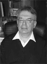
Our correspondent met with Vladimir Izyaslavovich Gavrilenko, Vice-Director of the Institute for Physics of Microstructures of the Russian Academy of Science, Head of semiconductor physics department with this institute, USSR State Prize winner, professor, Doctor of physical and mathematical sciences, for a good reason. Just days before the New Year’s eve, on 15 December 2011, he marked his 60th birthday. And the bigger part of his life right from the school bench has been devoted to science.
 Vladimir I. Gavrilenko was born in Gorky (Nizhny Novgorod). In 1966 our famed school No. 40 that for many years was headed by Veniamin Ya. Veksler extended admission of bright capable students. Volodya Gavrilenko was enrolled in the 8th grade as a physics contests -"olympiads'- winner. The physics teacher in that class was Nelly M. Zvereva, an excellent educator and a striking personality, and so physics became his favourite subject.
Says Vladimir Izyaslavovich: «When you are keen on something, it comes easier to you. I started by participating in school and regional olympiads and was lucky. After winning the first prize at the regional contest, I went on to take part in the 1st All-Union Olympiad that was held in the Moscow Institute of Physics and Technology (MIPT) in Dolgoprudny near Moscow. I got the first prize and fell in love with this institute — from then on I looked forward to studying physics only there'.
He graduated from MIPT in 1975. This higher school has a tradition of getting their graduate students engaged in research work at academic and departmental research institutes. V. I. Gavrilenko received his diploma from the  Lebedev Physical Institute (FIAN), where he also did his postgraduate studies. His scientific advisors were Viktor S. Vavilov, son of Sergey I. Vavilov, and Vladimir N. Murzin. In 1978, at 27, when he was already affiliated with the Institute of Applied Physics RAS, he defended his PhD thesis. Two years before completing the PhD course he got married. And it is natural that his scientific and private life has since been inseparable from the hometown. In 1993 a decision was made on establishing the Institute for Physics of Microstructures RAS in Nizhny Novgorod. By this act the Academy authorities acknowledged the world-level competence of the Nizhny Novgorod physicists in the fields of solid-state nanostructures, high-temperature superconductivity and x-ray optics. A convincing evidence of such recognition is that the institute was housed in a specially constructed building, which was an out-of-the-ordinary event in the early 1990s. V. I. Gavrilenko has been with the IPM RAS since 1994.
It should be said that even with the scientist’s comments it is rather difficult to understand what’s what in a research institute. We therefore take the liberty of straying from the main story to introduce the reader to the scope of problems of concern to the Department of semiconductor physics in addition to what its Head has to say.
Department of semiconductor physics is the largest of all departments in IPM RAS. There are over 60 employees including graduate and post-graduate students. The main trends of research activity include the physical foundations of development of silicon optoelectronics in the near-IR range and the problems of extending semiconductor nanostructures to the terahertz range.
V.I. Gavrilenko: «When I came back to Gorky and began working at the Institute of Applied Physics RAS, the topic of my research changed completely. It was a stressful situation for me. For a few years I did not have a single publication. But that I came from another place proved very useful. Nizhny Novgorod is renowned for radiophysics. I joined a strong research team that was working on a problem requiring experiments in pulsed electric fields. We had a lab in our division with highly competent radio specialists working in it. But, for some reason, they were unable to combine their knowledge with the hands-on experience. And I brought charts and drawings. I got down to soldering work and made a few devices that helped us start experimenting. Those experiments allowed us to discover effects that had never been observed before. Some groups in our division were engaged in a study of hot carriers in such relatively simple material as p-type germanium. I was directly involved in this work that resulted in creation of a new type of laser in the terahertz range and was awarded the State Prize.
The 1987 USSR State Prize for science and technology, «Inverted distributions of hot charge carriers in semiconductors and generation of stimulated emission in the millimeter, submillimeter and FIR ranges' (V.I. Gavrilenko is one of the twelve laureates). New physical effects arising by dynamic heating of charge carriers in semiconductors under strong electric and magnetic fields and causing substantial deformation of the distribution function, localization and accumulation of carriers in the selected areas of momentum space were predicted, discovered and studied in detail. Stimulated emission was for the first time produced in the inverted systems of hot holes in germanium, and world’s first laboratory models of semiconductor masers and lasers in the short-wave part of millimeter, submillimeter and far-IR (terahertz) ranges were developed.
V.I. Gavrilenko: 'The research was rapidly progressing and in 1984 two groups in our division succeeded in generating stimulated emission. In one group the effect was obtained in crossed fields, while Z.F. Krasilnik, myself and our colleagues observed it in parallel electric and magnetic fields. Unfortunately, those devices, although very interesting from the physical point of view, have not found practical application, again for some purely physical reasons. This work turned out to be textbook material.
In 1992 I defended my doctoral thesis. Since that time, when still at the Institute of Applied Physics, I began working on semiconductor quantum well heterostuctures on germanium and silicon basis. And all of my further research activities have been connected with the terahertz spectroscopy of semiconductor nanostructures'.
The idea of using structures with heterotransitions in semiconductor electronics was put forward in the early 1950s, at the dawn of electronics, but few took it seriously at the time. However, already in the late XX century the Nobel Committee thought it right to award a prize for the «fundamental work in the field of information and communication technologies'. It is this area of human activity that has seen major breakthroughs in recent decades. Says Zhores I. Alferov, Russian scientist, Nobel Prize winner:'The outstanding achievements in physics and technology of semiconductor heterostructures have led to remarkable changes in our daily life… We can hardly imagine our life today without telecommunication systems based on double heterostructure lasers, without heterostructure LEDs and bipolar transistors, without low-noise high electron mobility transistors used in high-frequency devices including satellite television systems'.
V.I. Gavrilenko: «Advancing research into the terahertz range is very important. As a matter of fact, there are no such wavelengths that would not be of use to man. Electromagnetic waves of the terahertz range are reflected by metals but they penetrate plastics, paper, dry wood and all sorts of turbid media and fine materials. The rotational spectra of many organic molecules, including fluctuations of biologically important collective modes of DNA and proteins lie in the terahertz range. There is, for example, such a problem as development of airport safety systems. The Japanese have for a few years already been using a system that «sees through' airmail. In the 1990s we found it hard to develop experimental research. We did not have the necessary equipment, people quit. It got easier when several groups at the Institute received support from the Soros foundation in 1994. The 20% overheads covered the purchase of office equipment for the all-institute service departments and wiring of the first computer networks. Our group had the largest project in Nizhny Novgorod region (about 100 000 USD). The topic of research was germanium-silicon structures. The project budget allowed us to buy computers and spare parts for the imported equipment. Yet, life once again showed that money is not everything. Of the team that was involved in the fulfillment of that project very few stayed at the Institute.
The problem of personnel is the most acute one, indeed. At IPM RAS we have a base faculty of the Lobachevsky State University of Nizhny Novgorod (NNSU), Physics of nanostructures and nanoelectronics, that offers training for students from all of the NNSU three physical departments. When students choose to specialize in IPM RAS, some courses on their university curriculum are replaced by the special courses taught at our faculty.
To have undergraduates clearly understand what they will do as senior students if they decide on our faculty for majoring in their special field, an experimental training-research program had been elaborated. For a few weeks third-year students are to work on their experiments at the institute labs where the main investigations are underway, side by side with the IPM researchers. Then they go to another lab and can do another experiment. In one term they manage to perform two or three experimental studies, and it does happen that some students ask for a permission to stay at the Institute another term. When the training-research experiment is over, we hold a conference for the students to share their learning experience with each other. Only afterwards they make a decision on where they will do their course work and later on the bachelor’s, master’s and, possibly, PhD research. Those students who have finally chosen our base faculty are supposed to participate in the students' conference as a mandatory form of reporting their progress. The conference is held once a semester, in December and May, and each student is to speak about his/her current work and achievements. Besides, we have a regular educational workshop for graduate and post-graduate students. It is quite popular with both graduates and mature scientists and is usually attended by 80-90 people.
Since the early 2000s young professionals started coming to the Institute and at first we took on nearly all. Now we are more demanding of personnel selection. Our prime consideration here is whether the young candidate is capable of a creative approach to science. There are many examples of brilliant university graduates who then proved unable to make it as a successful scientist.
Among those who stay with us there are no mediocrities. Аnd some are genuinely talented. Here is a recent example. A very gifted young scientist, Sergey Krishtopenko, on completing his postgraduate studies simultaneously in Russia and France, defended his PhD thesis at the University of Toulouse in November 2011. He came to IPM RAS as a third-year student and in the study of quantum mechanics he calculated the energy spectrum in narrow-band heterostructures we were then investigating. For the second time in my life I chose a theorist for a PhD student, and was right. Sergey went on providing theoretical background for our experimental tasks and in a short while advanced beyond the level of competence of the «adult\\' scientists in our institute. He is now affiliated with the IPM RAS. The Academy allocated four fixed wages to young scientists for a period of three years and one was given to S. Kryshtopenko as the only postgraduate to have presented his thesis immediately after the PhD studies. Last summer he inspired his young colleagues-experimentalists and together they discovered the spin resonance in 2D electron gas in InAs/AlSb quantum wells, that had been predicted by Sergey. It is a pioneering work'.
In terms of practical applications, the history of the semiconductor lasers development is largely the history of combatting their threshold currents to reduce the laser generation threshold. Indeed, high currents involve high dissipated powers and, consequently, overheating and fast deterioration of semiconductor structures. Low threshold currents ensure long-lived miniature laser devices. And, while classical heterostructures have expanded the technological horizons, the low-dimensional semiconductor heterostructures offer a virtually unlimited research, technology and engineering freedom. By adjusting a heterostructure parameters, researchers today can form structures with any desired properties.
The complicated growth and experimental techniques require considerable spending. Nevertheless, the current level of Russian science in this field is quite high.
V.I. Gavrilenko: 'My group of experimenters is engaged in the terahertz spectroscopy. To work successfully we primarily need world’s quality samples. The fundamental studies require low temperatures and high magnetic fields, and in this area we have not advanced far since the 1980s, which corresponds to the world’s level of the 60s. We have to do many things in foreign laboratories. Now there is an opportunity to purchase equipment. Last year we bought a cryostat with a superconducting solenoid magnet of 12T. Next year’s plans include the purchase of a helium liquefying refrigerator. We are also going to set up a collector of helium gas so it can be re-used.
In science I am interested in finding things that no one has ever seen before. And something new does turn up from time to time. Nothing can compare with the thrill of discovery I experienced when we got stimulated emission in germanium. I wish our students would advance farther in our science and never lose this ability to wonder and delight in research'.
The high creative potential, skillful handling of the soviet-time technological background, expertise and wide international cooperation allow the IPMRAS researchers to maintain the cutting-edge science standards.
Interviewed by M. Goryunova
